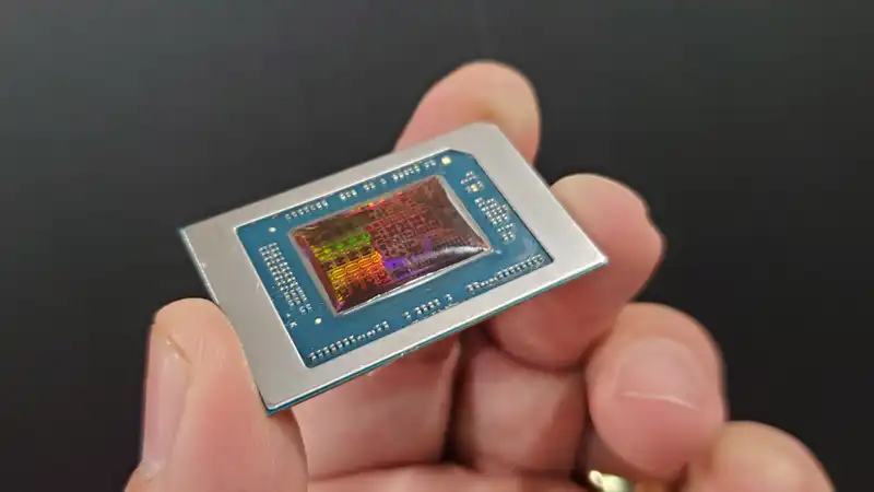
At an event in Los Angeles last week, AMD went into more detail about all the changes it is introducing with its Zen 5 CPU architecture. Although brief, the chip giant also described the new features of RDNA 3.5, or the “slight improvements” that have been “bolted on” to the current graphics processor design. In short, it is designed to optimize rendering performance for mobile applications.
The updated design was introduced by Mark Papermaster, AMD's CTO, who began by pointing out that the changes stemmed from a collaboration with Samsung, which has licensed AMD's graphics technology for its Exynos series of smartphones and tablet processors. He noted that the change was born out of.
“Many of the technologies are ideal for notebooks,” he said. These technologies are well suited to deliver the same great experience as Radeon graphics, but with less power consumption and higher efficiency.
While not a significant change, it is to be expected given the architecture's codename: RDNA 3.5 exists to remedy some of the performance bottlenecks that AMD's GPUs face when used in low-power, low shader count configurations.
In the latter case, these GPUs typically operate with a power budget of around 15W, and sometimes more, but still considerably less than the minimum power consumption of a discrete GPU. For example, the Radeon RX 6400 can use up to 54W, which is 80% more power than the Asus ROG Ally GPU can demand. This is 80% more power than the Asus ROG Ally GPU can demand.
Combined with the low number of compute units (CUs), this means that certain rendering operations that normally would not be a concern for a desktop GPU become limiting factors in overall performance. papermaster first identified the texture sampling rate.
In RDNA 3, each CU has four texture units, each of which can sample and return one bilinearly filtered texel per clock cycle. According to Papermaster, AMD doubled this number to eight with RDNA 3.5, and you may wonder why. Low-power integrated GPUs do not run as fast as discrete desktop chips, and coupled with the fact that they use system memory for VRAM, texturing is a fairly slow process for mobile GPUs.
By doubling the number of samplers, the chip can fetch twice as many texels per clock cycle, compensating for the lower core clock. Because of the enormous latency involved in texture sampling, insufficient VRAM bandwidth is not necessarily a problem. [However, according to AMD's presentation slides, this doubling is for “a subset of the most common texture sampling operations,” so it is not as clear-cut as doubling the number of texture units. When I eventually get my hands on an RNDA 3.5 GPU, I will delve into what actually doubled.
The other 2x performance improvement given is in vector heavy operations involving interpolation and comparison of values. These involve reading multiple data from a vector register file and their performance is affected by clock speed, so it makes sense to improve here. I don't believe these routines are a significant bottleneck for integrated GPUs at all, but AMD clearly feels they are.
Or it could have something to do with all the other changes implemented in RDNA 3.5 to improve memory management. iGPUs don't have the power budget to enjoy super-fast clocks and can't afford massive caches, so in the mobile world, memory operations of any kind in the mobile world, every cycle saved in memory operations of any kind is a good thing.
These include new instructions that detect whether a single-use write operation has been issued, skip it, and let the GPU move on to the next instruction. Writing data, especially to RAM, is very time consuming, but vector multiplication can be handled in a few cycles.
The method of batch processing primitives (groups of vertices that make up a shape) is fine-tuned to take better advantage of spatial locality. Since primitive data is naturally grouped in cache and RAM, when you perform an operation that generates a memory address to fetch data, there is a very high probability that the next address will also be the same primitive (aka spatial locality). Improving the management of all these means reducing the number of system memory accesses and address operations.
RDNA 3.5 also features better memory compression algorithms, and the iGPU's memory controller has been properly optimized for LPDDR5. Access to system memory for graphics routines is not only slow, but also very energy inefficient compared to caches.
To sum it all up, it means doing more with the same or less amount of energy, which is why AMD did a performance comparison between a Strix Point APU with RDNA 3.5 and an RDNA 3 Hawk Point. Specifically, the comparison was between the Ryzen AI 9 HX 370 and the Ryzen 7 8840U, both of which had an upper limit of 15W.
The new GPUs were about 32% faster in the previous generation 3DMark Time Spy benchmark and 19% faster in the lighter Night Raid test. While the numbers look impressive at face value, the HX 370 has 33% more CUs than the 8840U. While it is not known at what clock speeds the GPUs of these chips were running, the fact that one has significantly more shader units than the other is by no means undeniable.
However, it is worth doing to take the scores of the Strix Point chips as an overall view of their capabilities: running Time Spy and Night Raid on a ROG Ally set to 15W yielded results of 2,915 and 19,994, respectively. number of CPU cores No one knows at this point how much the number of CPU cores, shaders, and clock speeds are affecting the results, but at least it bodes well for gaming. [But at this point we are not convinced that the RDNA 3.5 update will have that much of an impact on gaming compared to the increase in CPU core and shader counts.
.
Comments