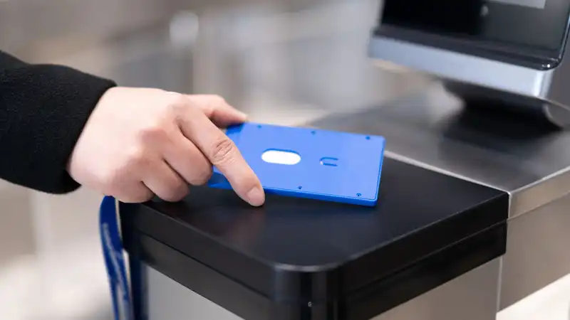
It does not require a battery. It doesn't even need to be connected to anything. Just wave it at a sensor to pay for goods or ride the subway or bus. nfc cards may seem to work by magic, but it's just good old-fashioned electronics. But as one prominent computer scientist discovered, the scale of what is happening is truly amazing. [Not only does he have a PhD in computer science and decades of experience working for Sun, Microsoft, Google, etc., but he also likes to explore the inner workings of chips by reverse engineering. x and on his blog, Sirif takes a look at Montreal subway travel cards, delved into how NFC (Near Field Communication) cards work. [The antenna picks up the 13.56 MHz radio signal from the sensor's transmitter and also provides a means to power the chip. All it needs is a small amount of energy from the radio waves. However, given that the processor (or rather the digital controller) is smaller than a grain of salt, it is not surprising that the power requirement is so small.
So small that Shirriff ran into all sorts of problems when he tried to remove it from the card, etch its layers, and see the logic circuitry inside. In his own words, "You just bump the chip or blow on it, and the chip may never be seen again."
Processor die images are phenomenal, and we have all looked at the work of someone like Fritschen Fritz and wondered. But this is on a whole other level. Not because it is made up of billions of transistors (it isn't) or because it is made at the most advanced process nodes (it isn't), but because we can see the individual transistors that make up the logic gates that process data.
Shirriff estimates that the chip is made at the 180 nm process node because the layers of transistors are slightly outside the limits of his optical microscope. Speaking of microscopic, the chip is tremendously small, measuring 570 x 485 microns (millionths of a meter) and 70 to 120 microns thick. Although rather silly, to put this in some context, more than 2,200 of them could fit inside the AD102 GPU used in the Nvidia GeForce RTX 4090.
It may seem somewhat ridiculous that these chips are manufactured for disposable use. After all, once a card wears out or becomes unacceptable, it is never recycled. But as Shirriff points out, NFC chip manufacturers like NXP Semiconductors don't sell individual chips; they buy entire silicon wafers that are manufactured at a cost of up to $12,000, depending on size. [Because that single wafer provides more than 200,000 usable dies, NFC card manufacturers are only looking at 6 cents per die, which is only a fraction of the cost of producing the entire card. Similar chips with more security features are used in contactless bank cards, hotel room "keys," and, of course, smartphones.
This particular chip consists primarily of circuitry that processes instructions carried by radio waves, along with a block of EEPROM (electronically erasable programmable read-only memory); it is the latter that stores the details accessed by the NFC sensor, in this case, remembering the travel details authorized by the cardholder. [Shirriff explains in detail what each part of the chip does, and the entire blog post is well worth reading.
Over the decades, we have gone from using magnetic strip PINs, through so-called smart chips, to using microscopic disposable silicone to pay for goods and travel in the public system. We take this for granted because of the skills of our engineers and scientists.
I have fond memories of tinkering with 741 op amps in the electronics lab in high school to make the lights glow with flair.
.
Comments