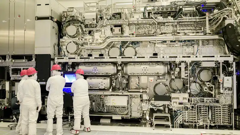
Making chips is tough. Really tough. Engineers could talk for hours about the complexity of a single step in the lithography or packaging process. But seeing is believing. A picture of Intel's new lithography "High NA EUV" machine shows just how complex chip manufacturing is.
What you see here is a lithography machine (incredibly, only one) called the TWINSCAN EXE:5000 High NA EUV. This $370 million machine will provide Intel with new capabilities to scale down processors to more efficient and effective designs; "High NA" stands for High Numerical Aperture; "EUV" stands for Extreme Ultraviolet; "EUV" stands for Extreme Ultraviolet; and "EUV" stands for Ultraviolet.
The broader chip manufacturing industry is adopting EUV for more continuous advances in chip manufacturing. The more miniaturized chips are, the more conventional DUV lithography processes require DUV processes that introduce extra steps into the manufacturing process, such as multi-patterning. This increases time, complexity, and cost. This is where EUV comes in, which again reduces the number of steps required while enabling process nodes below 10 nm. In theory, this would also reduce costs, but in practice this has not been the case; EUV requires very large and complex tools, as may be seen from the pictures below.
The important thing to note is that EUV does not change the fact that it is possible to make more complex and better performing processors. Intel is using EUV in the Intel 4 process node; TSMC has been using EUV since the N7+.
High NA EUV is also a bit different. By using new machines from ASML, a Dutch lithography machine manufacturer, Intel can produce wafers faster and improve yield per wafer. Mark Phillips, Intel Fellow and Director of Lithography Hardware & Solutions for Logic Technology Development, said that the increased resolution of the high-NA EUV will allow Intel to reduce the extra steps typically required for advanced chips, such as multi-patterning and the number of masks he said.
Overall, High NA is a simpler process, but the size and complexity of the machines required for it would not give that impression.
High NA EUV is not cheap. Intel must bear the burden of using these high NAs and using them effectively to get a return on investment.
"The introduction of high NA will continue in a few bottleneck layers, in parallel with layers that stay at 0.33 NA or what is called 193 [nm] immersion. Any cost-effective technology to achieve the needs of that process layer is acceptable"
.
Intel was the first company to get a High NA EUV machine, which will be used in the Intel 14A and later in the Intel 14A-E process nodes. Thus, it will be some time before we see Intel Core processors manufactured using High NA EUV.
Intel is on a mission to re-enter world-class chip manufacturing. To do so, it will need to leapfrog TSMC, the Taiwanese chipmaker that currently leads the world. Intel's plan to accomplish this includes "five nodes in four years," ultimately reclaiming the process leadership crown from TSMC in 2025 with Intel 18A. TSMC also wants to adopt High NA EUV, but has been slow to adopt this technology and instead choosing to focus on further patterning using its existing EUV process until much later.
According to press reports, at least one more High NA EUV machine has been sold to someone, but we do not know who. However, those people must have quite deep pockets.
Comments