Silicon is no longer our top transistor. We have had enough of your inability to maintain electrical properties on a micro scale. That's right, we are done with you. We are moving on to something better, something that can grow with us. Simply put, it is not us, it is you. We will probably have to change the name of that valley as well.
We have done really well with silicon, but companies like TSMC have been exploring alternatives (open in new tab) for some time, primarily as a way to try to keep up with Moore's Law. Moore's law observes that the number of transistors that can be manufactured on silicon doubles about every two years, while the cost of computers decreases
.
This law has been true for a long time, but is now going downhill; some companies, such as Nvidia, believe that Moore is almost dead (open in new tab), and AMD has stated that it is costly to keep pace with Moore (open in new tab). Regardless of where Moore's law stands today, the limits of silicon will likely cause it to collapse in the near future (open in new tab).
Thankfully, researchers at MIT (open in new tab) have discovered what may be our next transistor romance. To achieve such minuscule sizes, researchers are working with a material so thin it is called a 2D material. These delicate crystal sheets are as thin as a single atom. The idea is to begin integrating these perfect crystal structures into silicon wafers, the current industry standard.
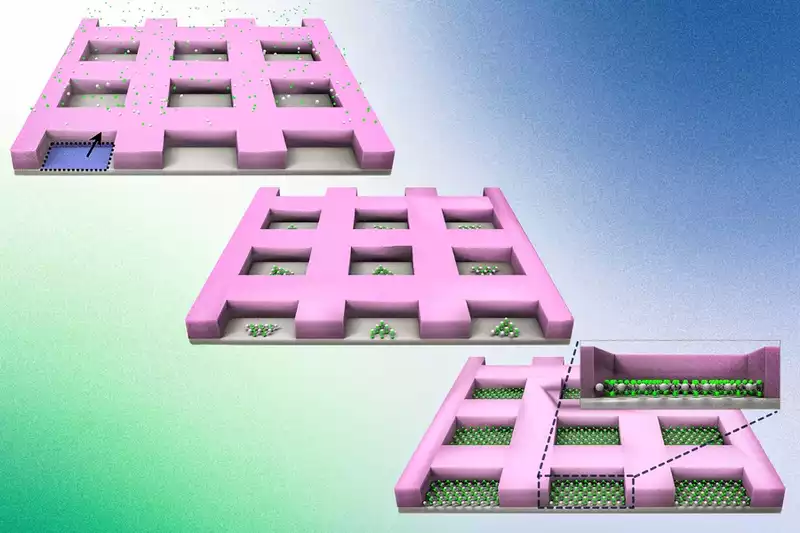
Until now, the delicacy of these 2D materials has been a major obstacle. The methods used usually involve peeling a small amount of material from a large amount of material, which is labor intensive, grows randomly, and sometimes leaves defects, so one has to look for the right part to peel.
Recently, a research team at MIT discovered a way to grow crystal sheets directly on silicon wafers. This process is called "non-pitaxial single crystal growth," and it seems to work.
So far, the team has successfully grown one of the two-dimensional materials, called transition metal dichalcogenides (TMDs), on silicon wafers in a crystal defect-free state. The team used this method to create simple but functional transistors and found that the 2D material works well on silicon wafers.
[14] "Until now, there has been no way to make 2D materials on silicon wafers in the form of single crystals. So the entire community has been struggling to realize next-generation processors without transferring 2D materials," explains Zee Hwan Kim, associate professor at the Massachusetts Institute of Technology (MIT). Now we have a way to solve this problem completely and make devices smaller than a few nanometers. This will change the paradigm of Moore's Law."The big question here, of course, is when we will see this technology. It will no doubt still need years of testing and trials, but it is an exciting proposition for the future. Because it can be built on the silicon infrastructure that already exists, this development has a better chance of becoming a mainstream product than many other developments. Furthermore, the future of computers looks crystal (open in new tab).
Comments